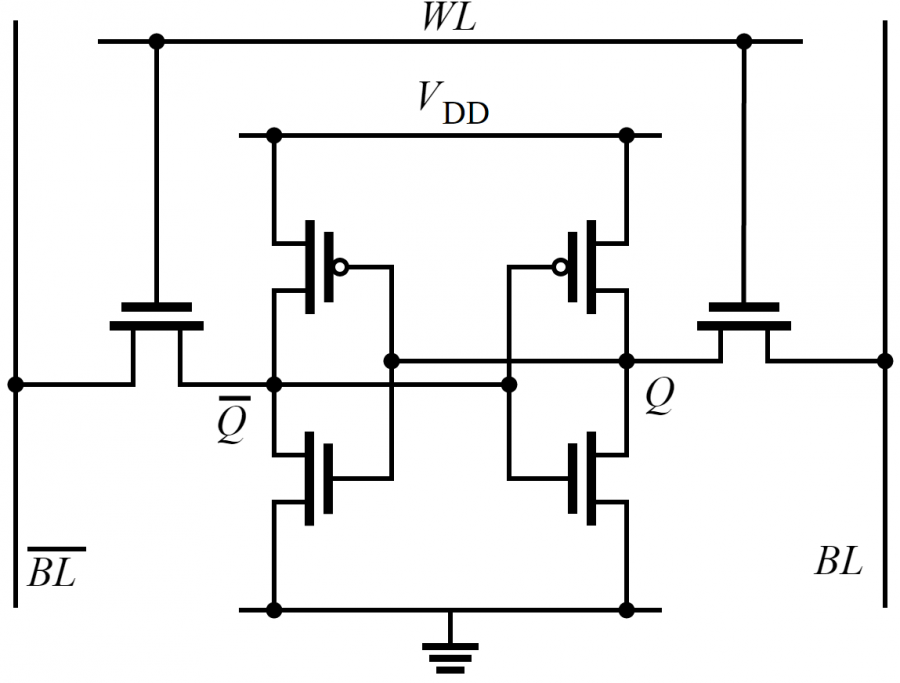
A SRAM Cell consists basically of 2 cross coupled CMOS inverters. By applying a logical 1 to the Wordline $$WL$$ the internal values become visible at the Bitlines $$BL$$. The Bitline $$BL$$ will have the value of the cell while the Bitline $$\overline{BL} $$ will have the complementary value. The reason is that if there is noise, the noise will influence both lines but will not change the voltage difference. Thats not the only reason, when writing a SRAM Cell we just can write a 0 and dependent on which side we do we set the value, this is due to the Vt drop at the wordline transistores. There are a lot more things to consider when dealing with SRAM Cells but as we are discussing the array architecture here I will skip this.
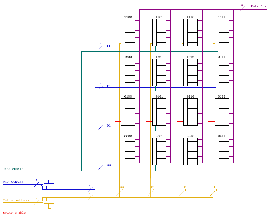
A sense amplifier will have both bitlines as input and will return a single bit which is representing the value stored in the cell. Memory arrays are organized as row and columns (like a table). Rows are accessed using the Wordline, Columns are accessed by selecting a Bitline. In order to select a row or column we need address encoders.

As you can see we have 3 bits for column addressing and 3 bits for row addressing. With 6 bits we can address $$2^6=64$$ SRAM-Cells (Bits). As you can see the SRAM architecture has a big transistor count, therefore it requires a lot of chip area and it also draws more power than eg. DRAM. But it is very fast and therefore used as Cache on the CPU of PCs. Also microcontrollers use SRAM as they usually do not have external RAM. The user is not interested in the internal architecture of the memory and also the user does not want to care about rows and columns. We simply define that the first 3 bits of the address define the row whereas the last 3 bits define the column. If we do so we end up with a table like this:
| 111000 | 111001 | 111010 | 111011 | 111100 | 111101 | 111110 | 111111 |
| 110000 | 110001 | 110010 | 110011 | 110100 | 110101 | 110110 | 110111 |
| 101000 | 101001 | 101010 | 101011 | 101100 | 101101 | 101110 | 101111 |
| 100000 | 100001 | 100010 | 100011 | 100100 | 100101 | 100110 | 100111 |
| 011000 | 011001 | 011010 | 011011 | 011100 | 011101 | 011110 | 011111 |
| 010000 | 010001 | 010010 | 010011 | 010100 | 010101 | 010110 | 010111 |
| 001000 | 001001 | 001010 | 001011 | 001100 | 001101 | 001110 | 001111 |
| 000000 | 000001 | 000010 | 000011 | 000100 | 000101 | 000110 | 000111 |
Read the page about multiplexers to learn more about how they work.
Memory Architectures with multi bit elements
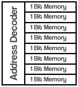
We are usually not interested in addressing single bits, dependent on the surrounding architecture the size of a single memory elements is usually 8/32/64 bit. We introduce a new symbol for a 8bit Memory element:
There are different ways on how to implement the Address Decoder. I want to discuss 2 possibilities here, the combinatorial and the 1 hot (MUX) approach.
Combinatorial Address Decoder
We can simply check if the current address on the bus is ours using a big end gate:
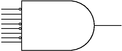
The AND Gate above would activate the memory element if the address is 01100101.
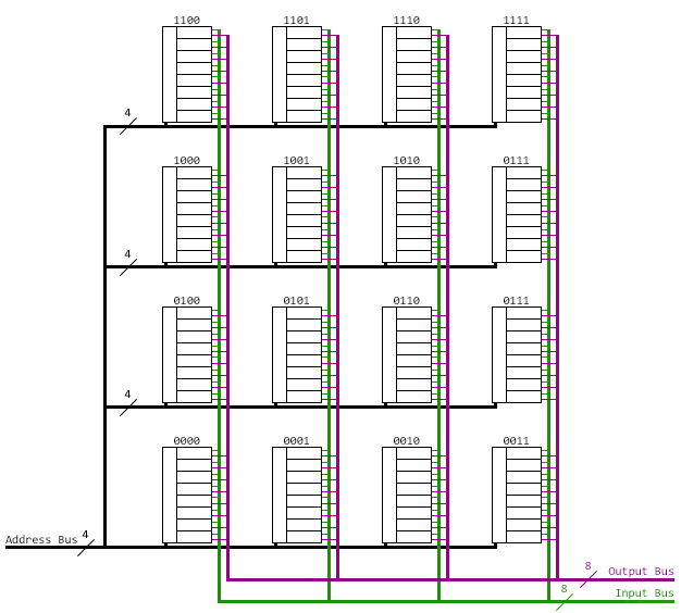
To keep the schematic simple I illustrated a memory array with 4 address bits and therefore 16 memory elements. Every memory element gets the complete address and need to decide if it is addressed or not. For big arrays this causes a big overhead and also comes with the drawback that every memory element needs another address decoder
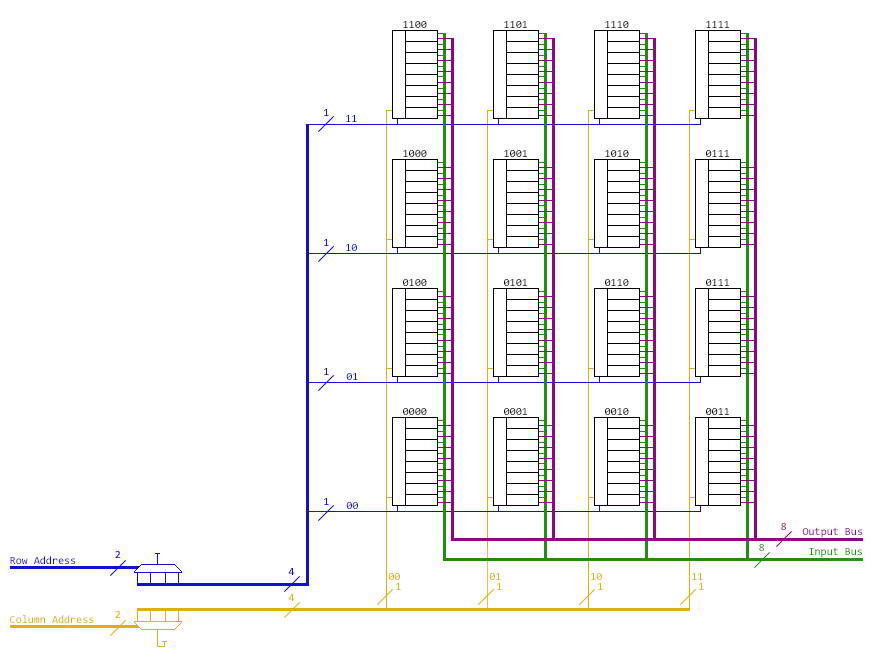
1 hot addressing
To overcome the issues with the combinatorial address encoding we can implement the 1 hot addressing which you already have seen with the SRAM Architecture. There are 2 address busses, one for the column and one for the row. Each of those busses has the same width as the original address and just one bit of each bus is allowed to be high at a time which means that we need to additional logic in order to generate those values but do not need complex address encoding inside the memory element as a simple AND gate is enough and all memory elements are now identical.
Bidirectional data lines
In the example above we had dedicated lines for input and output. Those lines can be combined to a bidirectional data bus. We need to make sure that we can switch the memory elements from read to write operation, therefore we need to introduce a switchable non inverting transmission gate:
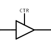
It is High Z (non conducting) if CTR is low and conducting if Z is high. However, we use this high level symbol for demonstration purposes, on transistor level things like this are unfortunately not that easy.
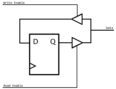
Additional we need to tell each memory element if it is in read or write state which requires additional wires.