Note
The underlying theory about current mirrors etc is skipped but might be added at some point.
Intro to Differential Amplifier Design
Differential amplifiers amplify a voltage difference at the input and are fundamental circuits in electronics. They are used in operational amplifier circuits and when ever a differential signal need to be amplified. Differential signals do have the advantage that they are immune to crosstalk and noise as those influence have no impact on the difference of this voltage levels. see SRAM technology.
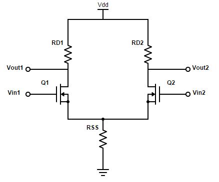
The principle is that a rising $$V_{in1}$$ will reduce the voltage at $$V_{out1}$$. This will reduce the voltage over $$Q2$$ and will lead to a lower current in the right path which is causing $$V_{out2}$$ to increase. We need a Resistor $$R_{SS}$$ to make sure that both Transistors stay in Saturation Region.
Key Parameters
Gain
The Overall gain consists of 2 parts, the differential gain $$A_{vD}$$ and the Common mode gain $$A_{vC}$$. Since we are interested to build up an differential amplifier, the common mode gain should be as small as possible.
The differential gain defines how much the voltage difference between $$V_{in1}$$ and $$V_{in2}$$ will be amplified whereas the common mode gain amplifies the input voltages itself (what we don’t want to happen):
$$V_{out1}-V_{out2}=A_{vD}(V_{in1}-V_{in2})\pm A_{VC}\frac{V_{in1}+V_{in2}}{2}$$
Common Mode Amplification
We can calculate the amplification if we connect both input pins together. As both Transistors and Resistors now work in parallel they the resistance is half of the original value whereas the transistors become twice as strong which means that we can double the Width/Length ratio.
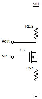
As you can see this is now a common Source stage.
The gain for a CS stage is
$$\left | A_{V}(CS) \right |= g_{m}R_{D}$$ from which we can derive the formula for our amplification.
$$\left | A_{vC} \right |= \tfrac{\tfrac{R_{D}}{2}}{\tfrac{1}{2\sqrt{}2µ_{n}C_{ox}\tfrac{W}{L}I_{d}}+R_{SS}} $$
You can see from that equation that an infinite $$R_{SS}$$ would lead to no common mode amplification as it would be an ideal current source.
Input Common Mode Range
As it had been discussed above the amplifier just works around an operating point. The range in which the amplifier works is defined as input common mode range (ICMR). We have linear dependency between the output voltages until one of the transistors leaves saturation. The INput common mode range is ~ 50% of $$V_{DD}-V{SS}$$
Offset
Transistors are not ideal because of several reasons during manufacturing therefore an 2 equal input values must not result in equal output voltages. We therefore add an Offset Voltage $$V_{OS}$$ to compensate this problem. $$V_{OS}$$ is usually in the range of 5-20mV.
$$V_{in1}-(V_{in2}+V_{OS})=V_{out1}-V_{out2}$$
Real amplifiers
In real live the difference of the input voltages is amplified and a voltage which is proportional to this difference is generated.
Note that $$V_{out}$$ is limited to $$V_{DD}$$ as upper bound and $$V_{SS}$$ as lower bound.
We also want to be able to amplify “negative” voltages, therefore we lower $$V_{SS}$$ to a negative value. We can achieve the same effect by adding an offset to the input voltages. However, if we do so we generate a new reference voltage, analogue ground which is 0V and in the middle between $$V_{DD}$$ and $$V_{SS}$$.
Making it single ended
We could change the circuit from fig1 in such a way that we just ignore one of the output voltage. The Problem with that is that both output voltages “move” in the opposite direction when the input voltage difference changes. By losing one of this voltages the gain would drop by 50%.
A better solution is to use a current mirror as pull up network.
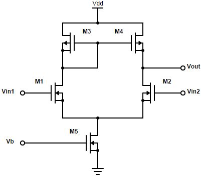
Lets say $$V_{in1}$$ is rising:
The current in $$M1$$ ( $$I_{D1}$$) is increasing while the current in $$M2$$ ( $$I_{D2}$$) is decreasing by the same value.
But at the same time the voltage over $$M3$$ is decreasing which is pulling gate node of the current mirror to ground. This will cause the currents in $$M3$$ and $$M4$$ to get bigger which is also causing the output voltage to rise.
Also you can see that I have replaced $$R_{SS}$$ by a NMOS. The reason is that resistors are difficult to manufacture on a chip. The bias voltage $$V_{b}$$ determines the “resistance” of this pull down network.
Calculations
$$I_{SS}$$
The current in $$M5$$ is the sum of the currents that go through $$M1$$ and $$M2$$
$$I_{SS}=I_{D1}+I_{D2}$$
gain
The small signal gain may be obtained from
$$i_{out}=g_{md}v_{ID}$$
where $$g_{md}$$ is the transconductance of the differential inputs.
$$v_{ID}=r_{out}i_{out}$$
where $$r_{out}$$ is determined my the $$M2$$ and $$M4$$
$$r_{out}=\frac{1}{g_{ds2}+g_{ds4}}=\frac{1}{(\lambda_{ds2}+\lambda_{ds4})\frac{I_{SS}}{2}}$$
we obtain (explanation on factors might be added in the future)
$$A_{v}=\frac{v_{out}}{g_{ds2}+g_{ds4}}=\frac{2}{\lambda_{2}+\lambda_{4} }\sqrt{K’_{N}{\frac{W_{1}}{L_{1}}\frac{1}{I_{SS}}}}$$
Input Voltage Range
As mentioned earlier $$M1$$ and $$M2$$ need to be in saturation, therefore the input voltages need to be in a certain range.
Investigation:
sweep the common mode voltage (inputs connected) [will be simulated later]
We have to find the highest and lowest possible input voltage for which $$M1$$ and $$M2$$ are in saturation.
For a single transistor we know that we need to fulfill $$V_{ds}\geqslant V_{GS}-V_{T}$$ to be in saturation region (and $$V_{GS}\geqslant V_{T}$$ of course)
Maximum voltage
The maximum common mode voltage is the same as the gate voltage at $$M1$$. It is $$V_{DD}$$ minus the voltage drop over Source to gate $$M3$$ plus the threshold voltage of $$M1$$.
$$V_{IC}(max)=V_{G1}(max)=V_{DD}-V_{SG3}-V_{DS1}+V_{GS1}=V_{DD}-V_{SG3}+V_{TN1}$$
Minimum voltage
$$M5$$ determines the minimum voltage as $$M5$$ also has to stay in saturation.
$$V_{DS5}=V_{IC}(min)-V_{SS}-V_{GS1}\Rightarrow V_{DS5}(sat)+V_{SS}+V_{GS1}\geqslant V_{IC}(min)$$
Slew Rate
The Slew rate determines how fast the output can charge or discharge a capacitive load $$C_{L}$$ at the output $$V_{out}$$. All internal parasitic contribute of course also to the Slew rate. However, $$M5$$ defines this attribute
$$SR={\frac{I_{5}}{C_{L}}}$$
3dB-frequency
We dither a constant input voltage (which is inside the ICMR) with a AC voltage. The 3dB frequency is the frequency of the AC voltage at which the output signal of this AC is only 70% percent. It is determined by the output resistance.
$$\omega_{-3dB}=2\pi f_{-3dB}=\frac{1}{R_{out}C_{L}}$$
Power dissipation
The power consumption is the voltage drop over the full circuit times the current in $$M5$$
$$P_{diss}=(V_{DD}-V_{SS})I_{SS}$$
Example Design
This example will be based on a 0.8µm Technology for which we have
| Parameter | Description | NMOS | PMOS | Unit |
| $$V_{th0}$$ | Threshold Voltage | $$0,5\pm 0,05$$ | $$-0,65\pm 0,05$$ | $$V$$ |
| $$K’$$ | Transistor-Transconductance | $$175\pm 10%$$ | $$60\pm 10%$$ | $$\frac{\mu A}{V^{2}}$$ |
| $$\gamma$$ | Bodyfactor | $$0,58$$ | $$0,42$$ | $$V^{\frac{1}{2}}$$ |
| $$\lambda$$ | Channel-length-modulation factor | $$0,06@L=1 \mu m$$ $$0,04@L=2 \mu m$$ |
$$0,06@L=1 \mu m$$ $$0,04@L=2 \mu m$$ |
$$V^{-1}$$ |
| $$2 \left | \phi_{F} \right |$$ | Surface potential for strong inversion |
$$0,8$$ | $$0,8$$ | $$V$$ |
Design Targets
Supply Voltage:
$$V_{DD}=3,3V$$
$$V_{SS}=0V$$
Slew Rate:
$$SR\geq20\frac{V}{\mu s}$$
3dB frequency
$$f_{-3dB}\geq200kHz(C_{L})=5pF$$
Input common mode range
$$0,75V\geq ICMR\geq 2,95V$$
Differential Amplification
$$A_{diff}=200$$
Power Dissipation
$$P_{diss}\geq 1mW$$
Calculation
$$I_{5}$$
The Slew Rate tells us how fast the load need to be charged/uncharged. As $$C_{L}$$ is given (5pF) we can calculate the minimum current $$I_{5}$$ (note that the Slew rate is given as Volts per µs and therefore needs to be multiplied)
$$I_{5}\geq SR*C_{L}= (20*10^{6}V)*(5*10^{-12}F)=100\mu A$$
The Power dissipation $$P_{diss}$$ is giving us the upper bound for $$I_{5}$$
$$I_{5}=\leq \frac {P_{diss}}{V_{DD}-V{SS}} = \frac {1+10^{-3}W}{3,3V}=303\mu A$$
If we also take the channel length modulation factors into consideration we have
$$r_{out}=\frac{1}{g_{ds2}+g_{ds4}}=\frac{1}{(\lambda_{ds2}+\lambda_{ds4})\frac{I_{SS}}{2}}\Rightarrow I_{5}=\frac {2}{(\lambda_{ds2}+\lambda_{ds4})R_{out}}$$
And by having knowledge about the 3dB frequency we can calculate $$R_{out}$$
$$\omega_{-3dB}=2\pi f_{-3dB}=\frac{1}{R_{out}C_{L}}$$
$$\therefore 2\pi 200kHz \leq \frac{1}{R_{out}5pF}\Rightarrow R_{out} \leq \frac{1}{2\pi 200kHz*5pF}=159k\Omega$$
With knowledge about $$R_{out}$$ we can set a lower bound which is considering the channel length modulation factor.
$$I_{5}=\frac {2}{(\lambda_{ds2}+\lambda_{ds4})R_{out}} = \frac {2}{(0,06+0,06)V^{-1}*159k\Omega}\approx 105\mu A$$
We now know $$100\mu A\leq105\mu A\leq I_{5}\leq 303\mu A$$
To have some margin we set $$I_{5}=200\mu A$$.
Designing the current mirror (ICMR max)
We need to determine the saturation current of $$M3$$ (and therefore also $$M4$$) to make sure that we have half of $$I_{ss} aka I_{5}$$ balanced on each side $$\frac{I_{5}}{2}=100\mu A$$
we know that
$$V_{IC}(max)=V_{G1}(max)=2,95V=V_{DD}-V_{SG3}-V_{DS1}+V_{GS1}=V_{DD}-V_{SG3}+V_{TN1}$$
therefore
$$V_{SG3}=V_{DD}-V_{IC}(max)+V_{TN1}=3,3V-2,95V+0,5V=0,85V$$
Now we can determine the size of $$M3$$ and $$M4$$, the current is
$$I_{D3}=\frac{1}{2}K’\frac{W_{3}}{L_{3}}(V_{GS3}-V_{TP})^{2}$$
Note that this is an PMOS device and that $$V_{GS}=-V_{SG}$$
$$100\mu A=\frac{1}{2}60\frac{\mu A}{V^{2}}\frac{W_{3}}{L_{3}}(V_{GS3}-V_{TP})^{2}$$
$$100\mu A=\frac{1}{2}60\frac{\mu A}{V^{2}}\frac{W_{3}}{L_{3}}(-0,85+0,65)^{2}$$
$$\frac{W_{3}}{L_{3}}=\frac{100\mu A}{\frac{1}{2}60\frac{\mu A}{V^{2}}(-0,85+0,65)^{2}}=\frac{W_{4}}{L_{4}}= 83,33$$
Designing the Pull down transistors M1 and M2
From the gain specification and from the knowledge about the currents we now can calculate the W/L ratio for M1 and M2.
$$A_{diff}=g_{m1}R_{out}=\frac{g_{md}}{g_{ds2}+g_{ds4}}=\frac{\sqrt{2\mu_{n}C_{ox}\frac{W_{1}}{L_{1}}}}{(\lambda_{n}+\lambda_{p})\sqrt{I_{ss}}}$$
$$\therefore \frac{W_{1}}{L_{1}}=\frac{(\frac{A_{v}(\lambda_{n}+\lambda_{p})\sqrt{I_{5}}}{2})^{2}}{K’}=\frac{(\frac{200(0,06+0,06)\sqrt{200\mu A}}{2})^{2}}{175\frac{\mu A}{V^{2}}}\approx 164,57$$
M5
From the ICMR we can calculate $$V_{DS5}$$
$$V_{DS5}(sat)+V_{SS}+V_{GS2}\geq V_{IC}(min)$$
$$\therefore V_{DS5}(sat)= V_{IC}(min)-V_{SS}-V_{GS2}$$
We first need to know $$V_{GS2}$$
$$I_{2}=\frac{\mu_{n}C_{ox}}{2}\frac{W_{2}}{L_{2}}(V_{GS2}-V_{TN})^{2}$$
$$\therefore V_{GS2}=\sqrt{\frac{100\mu A}{\frac{175\frac{\mu A}{V^{2}}}{2}164,5}}=0,583V$$
$$\therefore V_{ds5}(sat)=0,166$$
W/L ratio for $$M_{5}$$
$$I_{5}=\frac{\mu_{n}C_{ox}}{2}\frac{W_{5}}{L_{5}}(V_{DS5}(sat))^{2}$$
$$\therefore \frac{W_{5}}{L_{5}}=\frac{I_{5}}{\frac{\mu_{n}C_{ox}}{2}(V_{ds5}(sat))^{2}}=\frac{200\mu A}{\frac{175 \frac{\mu A}{V^{2}}}{2}(0,166V)^{2}}\approx 82.29$$
$$V_{gs}$$ for bias current mirror
$$I_{6}=I_{5}=\frac{\mu_{n}C_{ox}}{2}\frac{W_{5}}{L_{5}}(V_{GS6}-V_{TN})^{2}$$
$$V_{GS6}=\sqrt{\frac{200\mu A}{\frac{175\frac{\mu A}{V^{2}}}{2}82,29}}+0,5=0,666V$$
$$R=\frac{V_{DD}-V_{gs6}-V_{ss}}{I_{d6}}=\frac{3,3V-0,66V-0V}{200\mu A}=13,166k \Omega$$
Simulation
I use LTSPICE for the simulation.
Offset and transfer
First I want to check if the offset voltage and the transfer characteristics.
We set the negative input to analog 0V and sweep the positive input.
**differential amplifier offset and transfer characteristics
*voltages
VIN+ 	1P 	0 	DC 	1.65
VDD 	1 	0 	DC 	3.3
VIN- 	1M 	0 	DC 	1.65

*load
CL 		3 	0 	5P

*transistors
M3 		2 	2 	1 	1 	MODP 	W = 833.3U 	L = 10U
M4 		3 	2 	1 	1 	MODP 	W = 833.3U 	L = 10U
M1 		2 	1P 	5 	0 	MODN 	W = 1645.7U L = 10U
M2 		3 	1M 	5 	0 	MODN 	W = 1645.7U L = 10U
M5 		5 	7 	0 	0 	MODN 	W = 822.9U 	L = 10U

*current mirror for bias
M6 		7 	7 	0 	0 	MODN 	W = 822.9U 	L = 10U
RR 		1 	7 	13160

*transistor specs
.MODEL MODN NMOS VTO=0.5   KP=175U GAMMA=0.58 LAMBDA=0.06 PHI = 0.8
.MODEL MODP PMOS VT0=-0.65 KP=60U  GAMMA=0.42 LAMBDA=0.06 PHI = 0.8

.DC VIN+ 0.0 3.3 50U
.END

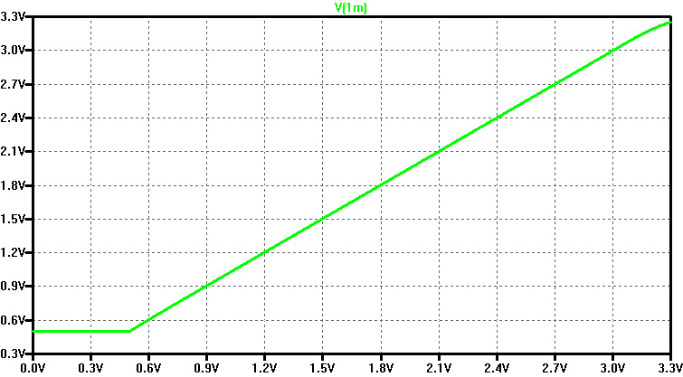
From the plot you can see that the supply voltage range is used from 0,9V to 3,1V
We do have an offset but as we are in the linear region this can be fixed by adding an offset voltage of about 3,5mV to the negative input.
It also can be seen that a 0,001V change of the input voltage results in a 0,2V difference at the output, so we have met our design goal for an Amplification factor of 200.
ICMR with unity gain configuration
Not we want to check the range of operation if we connect the output to the negative input and sweep the positive input.
**ICMR with unity gain configuration

*voltage
VIN+ 	1P 	0 	DC 	1.65
VDD  	1  	0 	DC 	3.3

*load
CL 		3 	0 	5p

*transistors
*dif ampf
M3 		2 	2 	1 	1 	MODP 	W=833u 	L=10u
M4 		1M 	2 	1 	1 	MODP 	W=833u 	L=10u
M1 		2 	1P 	5 	0 	MODN 	W=1645u L=10u
M2 		1M 	1M 	5 	0 	MODN 	W=1645u L=10u
M5 		5 	7 	0 	0 	MODN 	W=822u 	L=10u

*current mirror
M7 		7 	7 	0 	0 	MODN 	W=822u 	L=10u
RR 		1 	7 	13.166k

*transistor specs
.MODEL MODN NMOS VTO=0.5   KP=175U GAMMA=0.58 LAMBDA=0.06 PHI = 0.8
.MODEL MODP PMOS VT0=-0.65 KP=60U  GAMMA=0.42 LAMBDA=0.06 PHI = 0.8

*input sweep
.dc VIN+ 0.0 3.3 50u

.END
We can see that we have met our design goal of $$0,75V\geq ICMR\geq 2,95V$$
Bode Plot
In this configuration we want to see at which frequency the AC is not amplified anymore.
**bode plot
*voltages
VIN+ 	1P 	0 	DC 	1.65	AC	1.0
VDD 	1 	0 	DC 	3.3
VIN- 	1M 	0 	DC 	1.65

*load
CL 		3 	0 	5P

*transistors
M3 		2 	2 	1 	1 	MODP 	W = 833.3U 	L = 10U
M4 		3 	2 	1 	1 	MODP 	W = 833.3U 	L = 10U
M1 		2 	1P 	5 	0 	MODN 	W = 1645.7U L = 10U
M2 		3 	1M 	5 	0 	MODN 	W = 1645.7U L = 10U
M5 		5 	7 	0 	0 	MODN 	W = 822.9U 	L = 10U

*current mirror for bias
M6 		7 	7 	0 	0 	MODN 	W = 822.9U 	L = 10U
RR 		1 	7 	13160

*transistor specs
.MODEL MODN NMOS VTO=0.5   KP=175U GAMMA=0.58 LAMBDA=0.06 PHI = 0.8
.MODEL MODP PMOS VT0=-0.65 KP=60U  GAMMA=0.42 LAMBDA=0.06 PHI = 0.8

.AC 	DEC 50	1	 100MEG
.PRINT 	AC 	V(3)
.END

We have a -3dB frequency of around 355kHz which is better that the requirement of 200kHz so we also met this criteria.
Slew Rate
How fast can the capacitive load be charged and uncharged?
**Slew Rate

*voltage
VIN+ 	1P 	0 	PWL (0.0 1.0, 0.2U 1.0, 0.20001U 2.0, 0.8U 2.0, 0.80001U, 1.0)
VDD  	1  	0 	DC 	3.3

*load
CL 		1M 	0 	5p

*transistors
*dif ampf
M3 		2 	2 	1 	1 	MODP 	W=833u 	L=10u
M4 		1M 	2 	1 	1 	MODP 	W=833u 	L=10u
M1 		2 	1P 	5 	0 	MODN 	W=1645u L=10u
M2 		1M 	1M 	5 	0 	MODN 	W=1645u L=10u
M5 		5 	7 	0 	0 	MODN 	W=822u 	L=10u

*current mirror
M7 		7 	7 	0 	0 	MODN 	W=822u 	L=10u
RR 		1 	7 	13.166k

*transistor specs
.MODEL MODN NMOS VTO=0.5   KP=175U GAMMA=0.58 LAMBDA=0.06 PHI = 0.8
.MODEL MODP PMOS VT0=-0.65 KP=60U  GAMMA=0.42 LAMBDA=0.06 PHI = 0.8

.tran 0 1u
.PRINT TRAN V(1P) V(1M)

.plot V(3)

.END
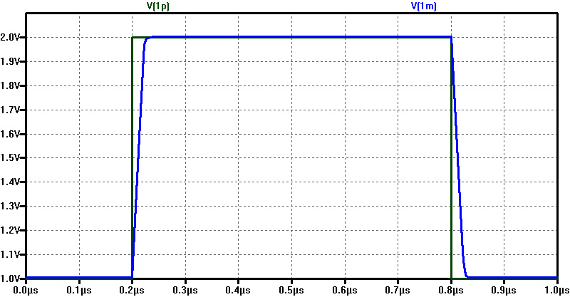
We can see that the leading and the trailing edge need ~30ns to reach the desired voltage, the slew rate therefore is (the $$10^{6}$$ is needed to bring it to the $$\frac{V}{\mu s}$$ scale
$$SR=\frac {1V}{30*10^{-9}V*10^{6}}=33.33\frac{V}{\mu s}\geq 20\frac{V}{\mu s}$$
so also the slew rate is better than our requirement.